ASSIGNMENT 5
RF SEMICONDUCTOR DEVICES AND USE IN SYSTEMS
RF semiconductor devices and methods of making the same are disclosed. In a disclosed method, a trench for defining an active region and an element isolation region is formed in a semiconductor substrate. One or more gate lines is then formed within the active region. Next, an insulating layer is formed on the semiconductor substrate and the gate lines. Contact holes are then formed in the insulating layer. Contact plugs are then formed in the contact holes. Thereafter, a conductive pattern is electrically connected with the contact plugs
RF Transistors
• BJT: low noise, linear power amplification,
power applications (bipolar operation)
• GaAs FET: very low noise, low power
(monopolar operation)
• HEMT (High electron mobility transistor):
very high frequency (f > 20 GHz)
(electron gas)

ASSIGNMENT 6
CELLULAR PHONE DIAGRAM SHOWING THE RF SECTION
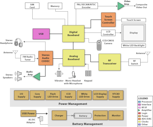
block iagram of a cellphone showing the RF tranceiver
http://electronics.howstuffworks.com/inside-cell-phone.htm

pictorioal view of an Ericson cellphone from ericson.com
No comments:
Post a Comment